
Method developed to make semiconductors smart, compact
Control Engineering
SEPTEMBER 9, 2022
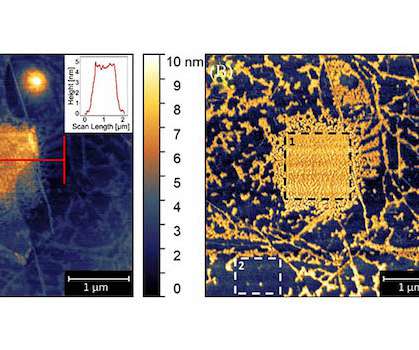
Using an electron beam, they are able to create a desired pattern on semiconductors — a technique not often used in the industry. Aligning patterns between processing steps makes the manufacturing process especially complex. They’re using an electron beam as a “pencil” to write the patterns exactly where they want them.


Let's personalize your content