
Method developed to make semiconductors smart, compact
Control Engineering
SEPTEMBER 9, 2022
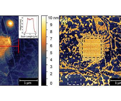
Using an electron beam, they are able to create a desired pattern on semiconductors — a technique not often used in the industry. Semiconductors are made of layers of thin films, each of which are deposited or etched with specific patterns that impact their functions. Semiconductor Insights.


Let's personalize your content